Machine Translated by Google
Preparation of organic thin films using a dip coater
Hiroshima University
There are various methods for fabricating organic thin films using solution techniques, such as spin coating and inkjet printing.
However, there are very few reports of the dip coating method.
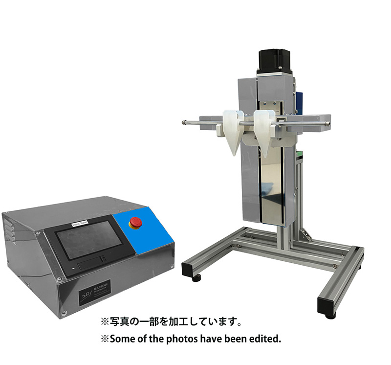
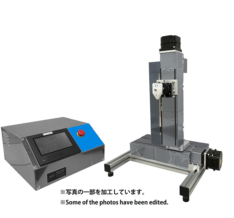
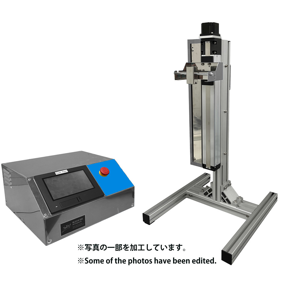
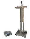
We report on the fabrication of organic thin films using a photocoater (manufactured by SDI Co., Ltd.).
The optimum conditions for fabricating the element were used as a reference. All thin films were untreated.
The device was fabricated on a non-crystalline n+-Si / SiO2 substrate.
•Dip coating method
The n+-Si / SiO2 substrate was immersed in a chloroform solution of C8-BTBT at 0.8 wt % (12 gL-1) at a speed of 10 mm/sec.
The substrate was then removed at a speed of 15 to 40 mm/sec.
After much trial and error, it was found that the sample should be placed in the solution at a speed of 10 mm/sec, immersed for 5 seconds, and then pulled out at a speed of 40 mm/sec.
It was possible to produce a thin film by repeating this series of processes about 10 times.
•Spin coating method
To compare the properties of the thin film prepared by the dip coating method, a thin film was prepared by the spin coating method as a reference.
The solution used was the same as that used in the dip coating method, and the spin coating conditions were 4000 rpm, 30 sec.
do.
(Figure 2).
The measurement results showed that the spin-coated film was a flat thin film of about 450 Å, whereas the dip-coated film had a clear thickness.
When the surface of the thin film was observed with a thickness gauge, the spin-coated film was found to be very flat.
In contrast, the surface of the dip-coated film was very uneven. This is because the crystallinity of C8-BTBT is high.
This is thought to be because the dip-coated film crystallized. The solution used in this study was very highly concentrated.
It is believed that the crystallization occurred due to the presence of the solvent. In the future, we will try to reduce the concentration of the solution or optimize the conditions such as the sweep speed.
It is speculated that this will enable the production of better quality thin films.
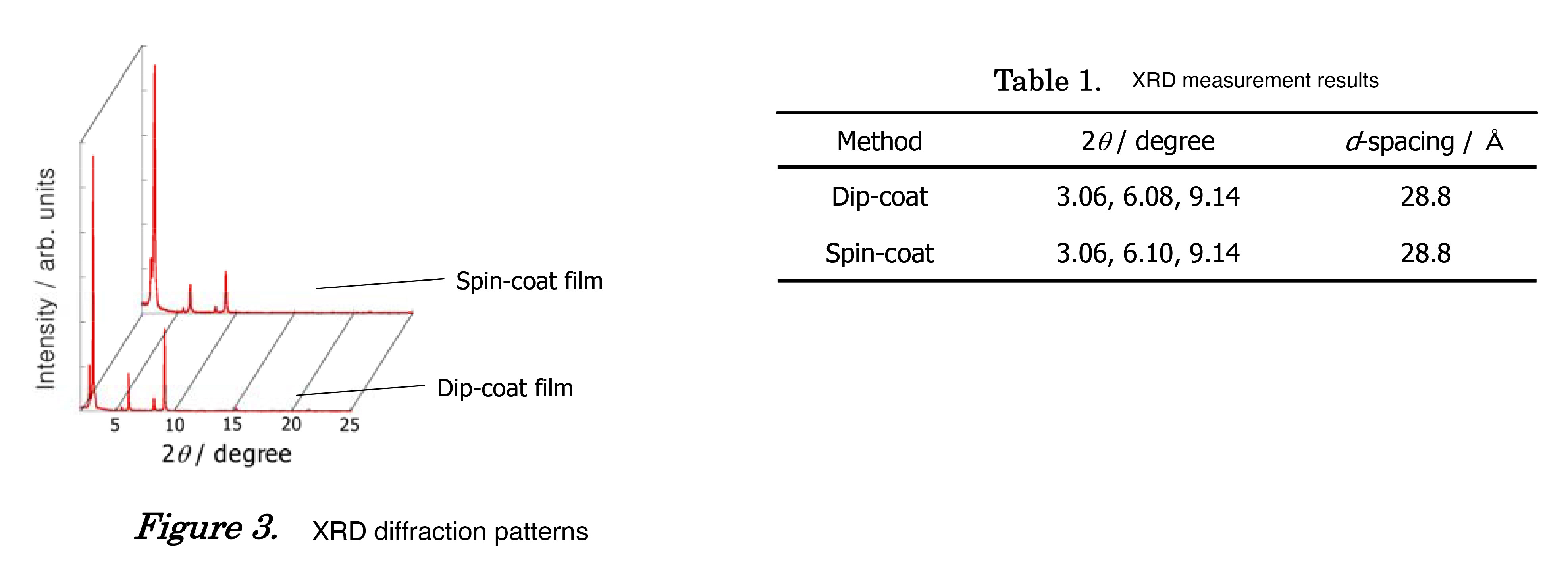 As a result of the measurements, it was found that the dip coating and spin coating methods
The same diffraction pattern was observed when either of these was used. This indicates that the molecular orientation of the thin film is in the out-of-plane direction.
It is thought that there is no significant difference.
The FET element had a top-contact structure as shown below, and measurements were performed in air, at room temperature, and in the dark (Figure 4).
The measurement results are shown in Figures 5 and 6 and Table 2.
Similar to the results in , the FET performance was almost the same and no significant differences were observed.
The film quality and FET performance were comparable for both. The film quality was further improved by optimizing the dip coating conditions.
It is believed that this can be done.
However, there are very few reports of the dip coating method.
We report on the fabrication of organic thin films using a photocoater (manufactured by SDI Co., Ltd.).

1. Thin film preparation
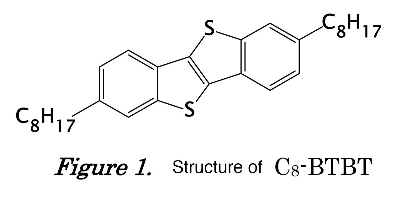
The material used in this study was C8-BTBT (H. 15732-15733), which is the most commonly Ebata J. Am. Soc. Chem. et al., used material in our laboratory. 2007, 129, (Figure 1) . The solution was prepared using the spin-coating method.The optimum conditions for fabricating the element were used as a reference. All thin films were untreated.
The device was fabricated on a non-crystalline n+-Si / SiO2 substrate.
•Dip coating method
The n+-Si / SiO2 substrate was immersed in a chloroform solution of C8-BTBT at 0.8 wt % (12 gL-1) at a speed of 10 mm/sec.
The substrate was then removed at a speed of 15 to 40 mm/sec.
After much trial and error, it was found that the sample should be placed in the solution at a speed of 10 mm/sec, immersed for 5 seconds, and then pulled out at a speed of 40 mm/sec.
It was possible to produce a thin film by repeating this series of processes about 10 times.
•Spin coating method
To compare the properties of the thin film prepared by the dip coating method, a thin film was prepared by the spin coating method as a reference.
The solution used was the same as that used in the dip coating method, and the spin coating conditions were 4000 rpm, 30 sec.
do.
2. Film thickness measurement and surface shape
The film thickness and surface shape of the thin film were investigated using a stylus film thickness gauge. The results are shown below.(Figure 2).
 (Left: Dip-coated film, Right: Spin-coated film)
The measurement results showed that the spin-coated film was a flat thin film of about 450 Å, whereas the dip-coated film had a clear thickness.
When the surface of the thin film was observed with a thickness gauge, the spin-coated film was found to be very flat.
In contrast, the surface of the dip-coated film was very uneven. This is because the crystallinity of C8-BTBT is high.
This is thought to be because the dip-coated film crystallized. The solution used in this study was very highly concentrated.
It is believed that the crystallization occurred due to the presence of the solvent. In the future, we will try to reduce the concentration of the solution or optimize the conditions such as the sweep speed.
It is speculated that this will enable the production of better quality thin films.
3. X-ray diffraction measurement (XRD measurement)
The thin films were subjected to XRD measurement, and the results are shown in Figure 3 and Table 1. As a result of the measurements, it was found that the dip coating and spin coating methods
The same diffraction pattern was observed when either of these was used. This indicates that the molecular orientation of the thin film is in the out-of-plane direction.
As a result of the measurements, it was found that the dip coating and spin coating methods
The same diffraction pattern was observed when either of these was used. This indicates that the molecular orientation of the thin film is in the out-of-plane direction.It is thought that there is no significant difference.
4. FET measurement
Finally, gold was evaporated onto the thin film through a shadow mask to fabricate a FET device, and its characteristics were evaluated.The FET element had a top-contact structure as shown below, and measurements were performed in air, at room temperature, and in the dark (Figure 4).
The measurement results are shown in Figures 5 and 6 and Table 2.

 (Left: Transfer characteristics (V d = -60 V), Middle: Hysteresis characteristics (V = -60 V), right: output characteristics)
 (Left: Transfer characteristics ( V d = -60 V), Middle: Hysteresis characteristics (V d = -60 V), right: output characteristics)

Similar to the results in , the FET performance was almost the same and no significant differences were observed.
5. Summary
The dip-coated film was a thin film with large irregularities compared to the flat spin-coated film.The film quality and FET performance were comparable for both. The film quality was further improved by optimizing the dip coating conditions.
It is believed that this can be done.
 Japanease
 English


