 Japanease
 English













September 29, 2025
Dip Coater Application Report: Formation of Aligned Carbon Nanotube Films
Ohno Laboratory, Department of Electronics, Graduate School of Engineering, Nagoya University
Haruki Uchiyama
1. BACKGROUND
Carbon nanotubes (CNTs) possess high carrier mobility and excellent electrostatic controllability, making them promising next-generation semiconductor channel materials capable of surpassing silicon. In particular, highly aligned semiconducting CNT arrays are essential for realizing Beyond 2 nm node integrated circuits because they can suppress short-channel effects while maintaining high drive capability. However, conventional chemical vapor deposition (CVD) methods struggle to simultaneously achieve high density and high purity, leading to device-to-device variability and degraded on/off ratios. Conversely, solution-based assembly of purified CNTs on substrates offers superior scalability to large-area substrates and guaranteed purity, but faces limitations in controlling uniform alignment and inter-tube spacing.
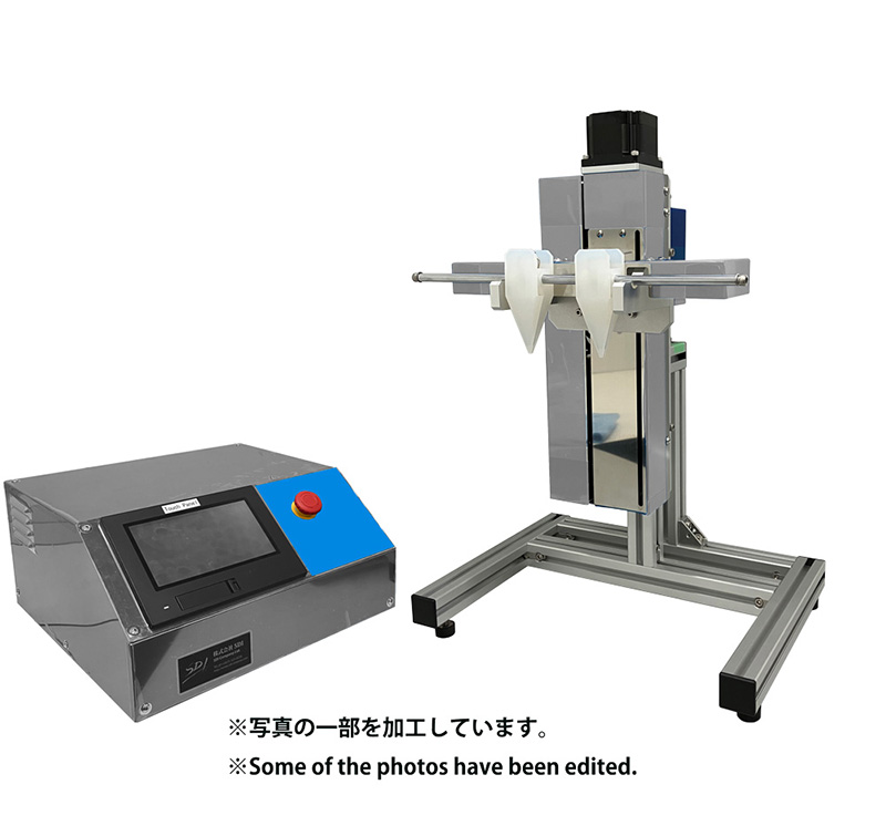
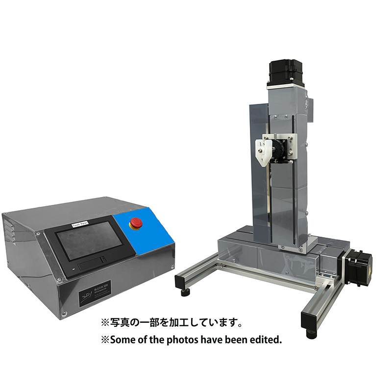
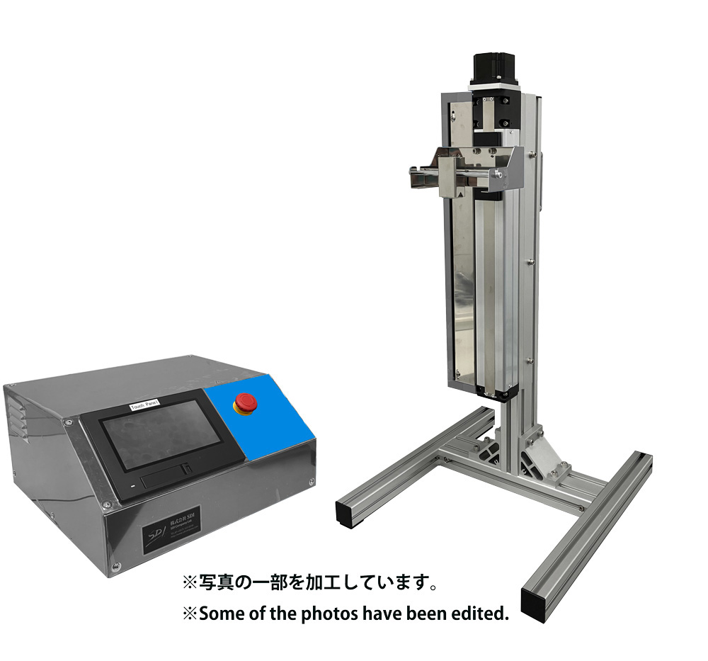
Recently, Liu et al. combined multi-step dispersion/purification with dimension-limited self-alignment (DLSA) to successfully deposit highly aligned CNT arrays with a semiconducting purity exceeding 99.9999% and a density of 100–200 CNTs/µm across an entire 4-inch silicon wafer [L. Liu et al., Science 368, 850 (2020)]. This milestone demonstrated the efficacy of self-aligning CNTs via a precise dip-coating withdrawal process. In this study, we attempted to form aligned CNT films using the dip coater (MD-0408-N1) and evaluated film uniformity and alignment.
2. EXPERIMENTAL
2.1 CNT Dispersion
Single-walled CNTs (EC1.5P, Meijo Nano Carbon) and a dispersing agent PCz (poly[9-(1-octyloctanoyl)-9H-carbazole-2,7-diyl]) (20 mg each) were dispersed in 10 mL of toluene. The dispersion was ultrasonicated in a sealed cell (40% power, 30 min) to yield a homogeneous CNT suspension.
2.2 Extraction of Semiconducting CNTs
The CNT dispersion was centrifuged (31,000 rpm, 50,000 g, 2 h). After centrifugation, 3.0 mL of supernatant was collected from each of 6 tubes, yielding a total of 18 mL of semiconducting CNT solution.
2.3 Removal of Impurities
The semiconducting CNT dispersion was vacuum-filtered through a PTFE membrane filter (Millipore, 200 nm) to remove free polymer and short CNTs. The CNTs retained on the filter were redispersed in THF (100 mL) via sonication (40 W, 6 min), followed by centrifugation (20,000 rpm, 20,000 g, 20 min) to extract the supernatant.
2.4 Alignment via DLSA (Figure 1)
The extracted solution was redispersed in 20 mL of 1,1,2-trichloroethane and filled into a quartz vessel (5 cm × 1 cm × 4.5 cm). A Si substrate (2 cm × 2.5 cm) was immersed vertically into this solution, and 20 µL of 2-butene-1,4-diol was dropped near the substrate. Utilizing the interfacial layer formed at the solution surface, the dip coater (MD-0408-N1) withdrew the substrate at a constant speed (1 µm/s) to self-align the CNTs on the substrate.
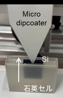
Figure 1. DLSA experimental setup showing the dipcoater, Si substrate, and quartz cell.
3. RESULTS
Figure 2 shows AFM images of the fabricated DLSA CNT film: (a) wide-area scan (scan size: 20 µm) and (b) magnified scan (scan size: 5 µm). The wide-area image reveals that while CNTs are distributed over the entire surface, low-density regions exist locally, highlighting an issue with film uniformity. The magnified view confirms that CNTs are aligned along a preferred direction, though partial meandering is observed. Granular features on the film are attributed to process residues such as residual polymer. These results demonstrate the effectiveness of DLSA alignment while indicating that improving uniformity and cleanliness remains a key future task.
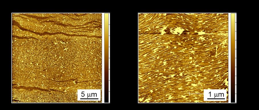
Figure 2. AFM images of DLSA-deposited CNT film: (a) 20 µm scan, (b) 5 µm scan.
4. SUMMARY
In this study, aligned CNT films were fabricated via DLSA using a dip coater. AFM observation confirmed the formation of aligned CNT structures on the substrate, though challenges such as insufficient film uniformity, meandering alignment, and residual impurities were also revealed. Future work will focus on optimizing CNT concentration and substrate withdrawal speed, as well as advancing washing and purification protocols to achieve clean, highly aligned, and uniform CNT films.
5. REFERENCES
1) L. Liu et al., Aligned high-density semiconducting carbon nanotube arrays for high-performance electronics. Science 368 (2020) 850–854.